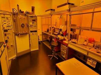
Lab thin film technology
High-vacuum equipment with various PVD technologies for thin-film technology is available in the microtechnology laboratory. In addition to the coating processes of resistance evaporation, electron beam evaporation and magnetron sputtering in DC, HF and reactive, sputter etching is also available for substrate pre-treatment and structuring. The sources are optimised for uniform coating on a wafer size of approx. 100mm.
The following process steps are spin coating for photoresist application and mask alignment for aligning and exposing the substrate with a photomask. Following this, the applied layer can be structured by wet chemical or sputter etching.
Thus, a complete process chain of mask technology is available.
A minimum structure width of 2µm is possible.
Available materials are chrome, chrome-nickel titanium, aluminium, silver, copper, aluminium oxide and glass.

